


Use High-Current IGBT Drivers with Built-In Protection for Reliable Industrial Motor Control
 In an ongoing effort to reduce costs and lower energy consumption in industrial control applications, designers are turning to high-frequency, high-current brushless direct current (BLDC) motors. These increasingly rely upon faster insulated-gate bipolar transistors (IGBTs) instead of metal-oxide-semiconductor field-effect transistors (MOSFETs) for faster switching in order to boost power density. However, to operate efficiently and safely, designers need to include buffer circuitry between the BLDC motor controller’s output and the IGBT power transistors.
Discrete circuitry comprising bipolar junction transistor (BJT) “totem-pole” circuits can perform this buffering role, but such solutions typically lack protection against high-voltage and high-current transients. They also aren’t able to level shift the digital controller’s low-voltage output to the higher voltages and currents needed to properly drive IGBTs. Adding this circuitry also complicates and slows down the design process, consumes space, and adds to the bill of materials (BOM).
To address these issues, a new generation of integrated high-frequency gate drivers for BLDC motor applications combines the buffer and boost circuitry needed to drive IGBTs, while also incorporating protection circuitry. Along with features to boost efficiency, these devices require fewer peripheral devices and have lower operating temperatures. Their smaller footprint further increases a high-frequency motor’s power density and saves space.
This article will briefly cover more driver basics, describing the role of high-current IGBT drivers in modern industrial electric motor applications. It then explains what to look for in an industrial grade device in order to maximize protection and efficiency while minimizing cost and complexity. Along the way, the article introduces sample drivers from ROHM Semiconductor, Texas Instruments, and ON Semiconductor, and discusses how to effectively incorporate them into a motor design.
BLDC motor driver basics
A common type of electric motor is the three-phase DC type in which rotor movement is induced by the rotating magnetic field generated by energizing the windings in a controlled sequence (commutation). The rotor speed is proportional to the motor’s operating frequency. Pulse-width modulation (PWM) is superimposed on the base operating frequency to control start-up current, torque, and power.
High-frequency operation offers some inherent advantages. For example, current ripple—an artifact of the alternating current (AC) input after rectification—is reduced, which in turn reduces the size and cost of the passive components needed for filtering. High-frequency operation also reduces the uneven electromotive force (EMF) that can result from a less-than-perfect sinusoidal input to the motor coils—decreasing motor vibration and wear. In general, higher frequency switching increases power density, allowing the use of physically smaller motors for a given output power.
Although there are variations, a typical closed loop control system for high-frequency operation comprises:
-
A speed control input, a controller that supervises motor commutation by generating the appropriate PWM to the driver
-
A driver that switches the low- and high-side power transistors
-
Power transistors, in a half H-bridge topology, which energize the motor coils
In a sensor-controlled BLDC motor, the control loop is closed via feedback from Hall effect sensors monitoring the motor’s rotating shaft (Figure 1). Sensorless models calculate motor position from back EMF (BEMF).

Figure 1: Typical closed loop control system for a three-phase BLDC motor comprising a controller, driver, and power transistor half H-bridge. This control system uses Hall effect sensors for the feedback circuit, though sensorless systems are also popular. (Image source: Texas Instruments)
The driver is a key component in a BLDC motor controller design. It is essentially a power amplifier that accepts a low power input from the BLDC motor controller and in turn produces a high-current drive input for the gates of the high- and low-side power IGBTs in the half H-bridge. That said, the latest versions of drivers for high-frequency operation are highly integrated and can do much more.
Advantages of integrated IGBT drivers
It is possible to build an IGBT driver from discrete components. Shown is a bipolar junction transistor (BJT) “totem-pole” circuit designed for driving a power transistor (Figure 2). In this case a more traditional MOSFET is used, but the configuration is applicable to an IGBT.
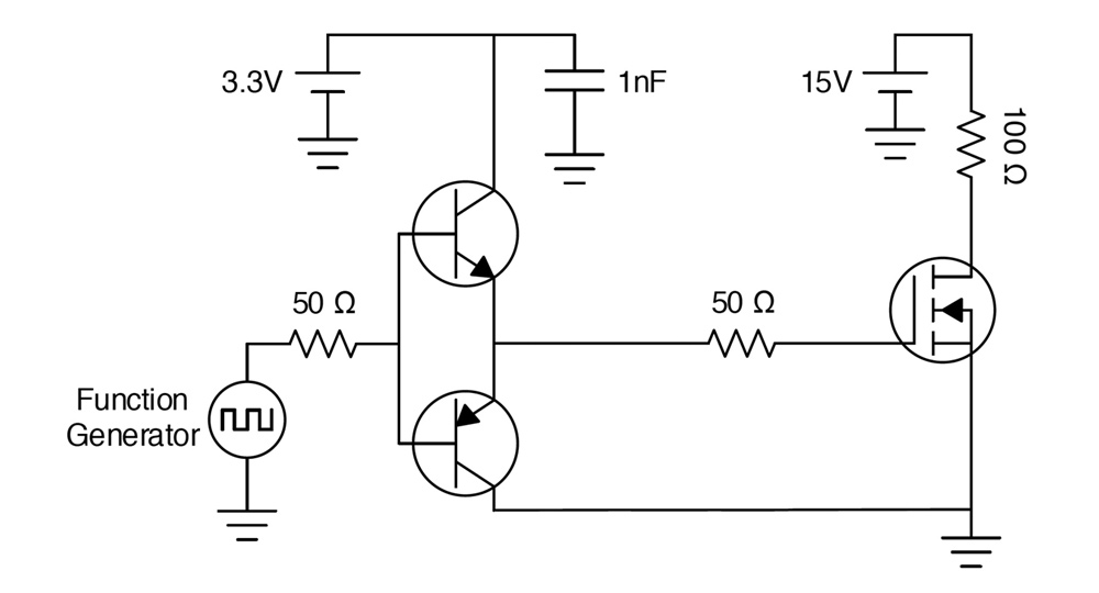
Figure 2: A discrete BJT totem-pole MOSFET driver works well but it inverts voltage, suffers from shoot through, and lacks protection. (Image source: Texas Instruments)
Two key disadvantages of this circuit are an inverted voltage at the output and some shoot through during gate voltage transients. In addition, at power on and power off (before the BJT drive supply reaches full operating voltage), the IGBT can be subject to the combination of high voltage and high current. This increases power dissipation and can cause overheating and permanent damage. While it is possible for the designer to add protection circuits required to meet the safety standards demanded of industrial BLDC motors, the design is challenging, and the additional components increase cost, complexity, and size.
Another issue with discrete BJT totem-pole circuits is a lack of level shifting. Digital power control now dominates BLDC motor control but offers only a low current/voltage output. For example, the PWM signal from the digital controller is often a 3.3 volt logic signal, which is not capable of effectively turning on an IGBT. Level shifting is required to raise the low current/voltage PWM signals from the controller to the high current/voltage PWM signals (typically 9 to 12 volts) required to activate IGBTs.
Apart from obvious advantages such as reduced design complexity, compressed development time, and smaller size, integrated high-current IGBT drivers address all the problems of a discrete solution. The devices also minimize the effect of high-frequency switching noise by locating the high-current driver physically close to the power switch while reducing power dissipation and thermal stress in the controllers.
For example, a solution such as ROHM Semiconductor’s BM60212FV-CE2 integrated gate driver is ideal for driving a pair of high- and low-side IGBTs. The device is compatible with either 3.3 or 5 volt controller logic signals while providing a high-side floating supply voltage of up to 1200 volts and a maximum gate drive voltage of 24 volts. Maximum turn on/off time is 75 nanoseconds (ns). The maximum output current is 4.5 amperes (A) (with a peak of 5 A for 1 microsecond (µs)).
Built-in protection
The new generation of IGBT drivers such as the BM60212FV-CE2 include built-in protection circuits, primarily undervoltage lockout (UVLO) and desaturation protection (DESAT).
UVLO is useful for avoiding overheating and damage during switch on. When turning on, if the gate voltage (VGS for a MOSFET or VGE for an IGBT) is too low, there is a danger of the transistor quickly entering its saturation region where conduction losses and power dissipation escalate. An illustration of this effect shows how values of VGS impact a power transistor (Figure 3). Again, a MOSFET is used for illustration purposes, but similar characteristics apply to the IGBT. The right side of the red curve is the saturation region, defined by a constant drain-to-source current (or collector-to-emitter current for the IGBT), dependent on VGS and independent of drain-source voltage (VDS).
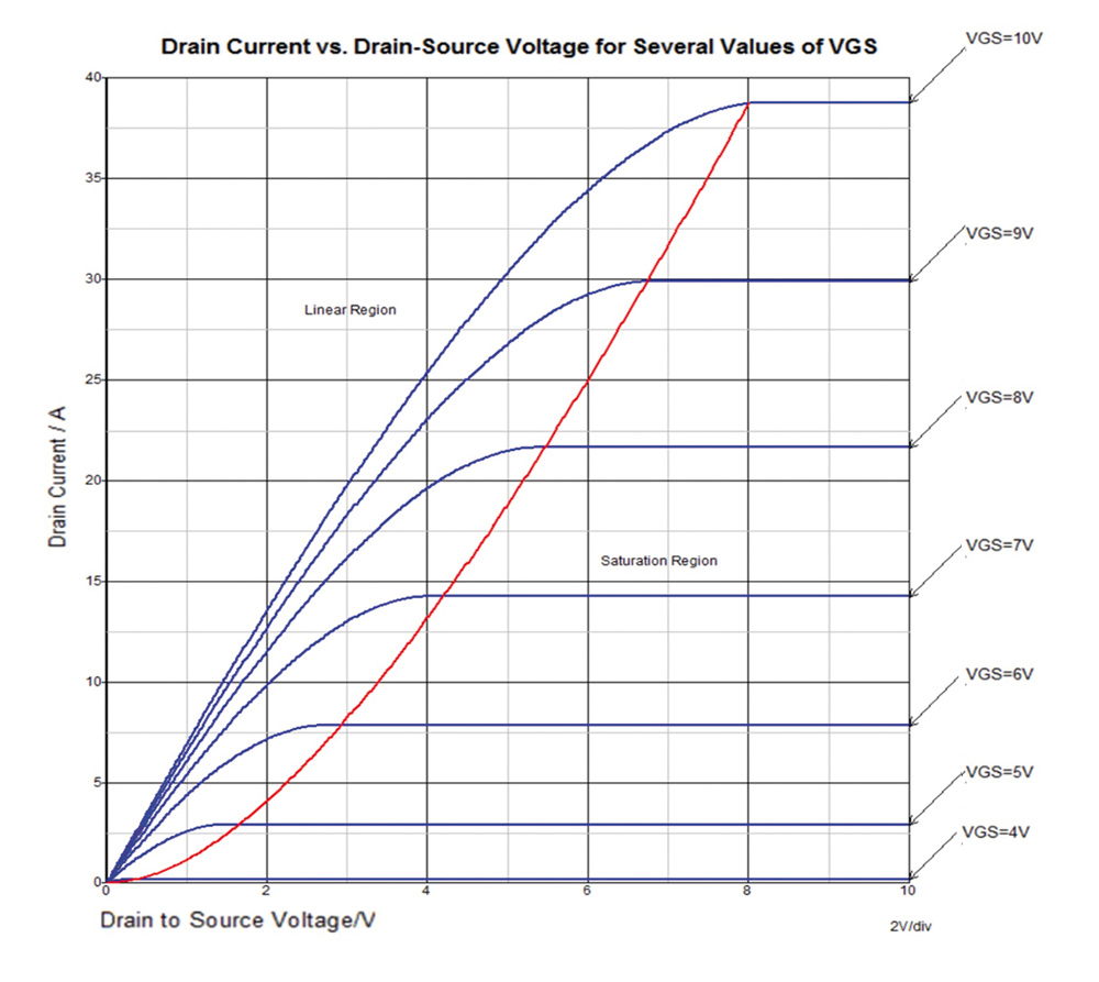
Figure 3: Losses escalate if the MOSFET or IGBT enters the saturation region (on the right of the red line) before fully switching on. (Image source: Texas Instruments)
The solution is to incorporate UVLO such that no voltage is applied to the gate until the power supply has reached a sufficient voltage level to ensure that the MOSFET or IGBT can be quickly turned on, and thus avoid excessive power dissipation. Texas Instruments’ UCC27512MDRSTEP IGBT (and MOSFET) gate driver, for example, includes a UVLO mechanism that grounds the output of the driver when the power supply has not reached a UVLO threshold determined by the designer (Figure 4). The UCC27512MDRSTEP is a low-side gate driver offering a peak sink current of 8 A.
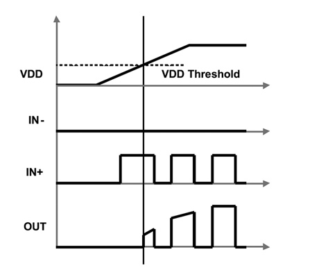
Figure 4: IGBT drivers such as TI’s UCC27512MDRSTEP include UVLO to ensure that the driver doesn’t start switching the IGBT until the power supply reaches a threshold. (Image source: Texas Instruments)
ON Semiconductor’s NCV5702DR2G is typical of IGBT drivers with a DESAT feature. This protection circuit compares the IGBT’s collector-emitter voltage (VCE) with a reference voltage. If it is higher the IGBT driver shuts down its output to protect the power transistor.
The NCV5702DR2G is a high-current IGBT driver designed to drive a high- and low-side pair of IGBTs in a motor drive application. The device can provide up to a 22 volt output from a -0.3 to 5.5 volt input. Peak sink current is 6.8 A (13 volts output) while peak source current is 7.8 A (-5 volt output voltage).
The NCV5702DR2G monitors the IGBT’s VCE once the device is fully turned on; in normal operation VCE should be around 3 volts for modern IGBTs. If the VCE is appreciably higher, it tends to indicate an overcurrent or similar stress event, which could potentially damage the IGBT.
For a short time at start up, VCE is typically high (only settling to the lower level after around 1 µs), so to prevent the DESAT protection from operating too early, the comparison with the reference voltage is delayed by a “blanking time,” which is set by a capacitor CBLANK (Figure 5).
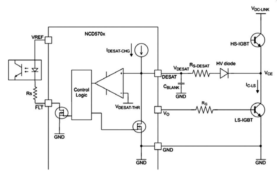
Figure 5: The DESAT protection circuit in the ON Semiconductor NCV5702DR2G IGBT driver switches off the output to the IGBT if VCE rises above a reference voltage VDESAT-THR. CBLANK sets a time delay to ensure DESAT protection doesn’t occur before the IGBT is fully turned on. Note: ON Semiconductor uses NCD570x for reference purposes in the datasheet. (Image source: ON Semiconductor)
In addition to their protection circuitry, integrated IGBT drivers offer superior performance to drivers constructed from discrete components because they typically include functions to boost efficiency.
Maximizing efficiency
BLDC motor power density is in part determined by efficiency; a BLDC that dissipates more power will require greater thermal management including larger heatsinks, increasing the size of the solution.
The losses generated during transistor switching are categorized as either static or dynamic. Static losses are generated by parameters such as the device’s parasitic resistance, while dynamic switching losses are, in part, due to parasitic capacitance.
During switching, the power dissipation of the transistor is proportional to the supply voltage, gate charge (QG), and switching frequency. For a given supply voltage, raising the switching frequency to increase power density must be countered by a reduction in QG if efficiency is not to be compromised.
A major contributor to an IGBT’s QG is parasitic capacitance, and a major part of that is the Miller capacitance. While the Miller effect was first identified in triode valves, it also affects modern transistors and manifests itself as an increase in overall input capacitance due to amplification capacitance between the input and output terminals during phases of the switching cycle. In addition to increasing QG, it is a major factor in limiting the gain of transistors at high frequencies.
Miller capacitance is most significant when the transistor is operating in the so-called Miller plateau region. In this region, the gate voltage remains constant (typically around 10 volts) while the gate drive current charges or discharges—depending upon whether the IGBT is switching on or off. If the driver can be configured to provide a high drive current at the Miller plateau, it can significantly reduce the duration of the phase and help reduce switching losses.
By providing a high current at the Miller plateau, IGBT drivers such as the ON Semiconductor NCV5702DR2G and ROHM Semiconductor BM60212FV-CE2 shorten the Miller plateau and ensure switching is more tightly controlled. Specifically, the high-current drive results in reduced turn-on energy (EON) during IGBT switching, which helps limit power dissipation. In addition, the high IGBT driver current, generated by the IGBT driver’s low-impedance internal FETs, ensures that even at high switching frequencies the power dissipation from the drive circuit is primarily across the external series resistor; and is therefore more manageable from a thermal perspective.
The Miller effect can also increase losses in the low-side IGBT switching. The problem occurs when switching on the high-side IGBT causes a voltage surge (dv/dt) on the collector of the switched-off low-side IGBT. The voltage surge induces a Miller current through the Miller capacitance to the gate capacitance of the low-side IGBT (Figure 6(a)). If the path from gate to ground (GND) has a critical impedance (caused by gate resistor RG), the Miller current could push the gate voltage above the threshold level and the low-side IGBT could be turned on for a few tens or hundreds of nanoseconds, increasing switching losses. One way to avoid this situation is to implement a negative gate voltage, but the downside is that this requires a second DC source.
An alternative is to provide a low-impedance path from gate to GND. Drivers like the NCV5702DR2G and BM60212FV-CE2 offer “active Miller clamp protection,” which implements this type of protection by adding a trace from the gate of the IGBT to the Clamp pin of the gate driver. Once the voltage output (VO) sinks below the active Miller clamp threshold (VMC-THR), the Clamp pin is shorted to GND and prevents the voltage on the gate of the IGBT from rising above the threshold voltage and switching the low-side IGBT (Figure 6(b)). The Clamp pin is disconnected from GND as soon as the IGBT turn-on signal is received at the gate driver input. Because the Clamp pin is engaged only after the gate voltage drops below the VMC-THR threshold, it ensures that the function of this pin does not interfere with the normal user controllable (via choice of RG) turn-off switching performance.

Figure 6: The Miller effect can increase losses in the low-side IGBT when the high-side IGBT causes a voltage surge in the switched-off low-side IGBT. The surge induces current through the Miller capacitance to the gate capacitance of the low-side IGBT (a). The solution (b) is to short the clamp pin to GND to prevent the voltage rising enough to turn the low-side IGBT on. (Image source: ON Semiconductor)
Design considerations for IGBT drivers
Even with a high-performance integrated IGBT driver, there are some challenges to overcome if the designer is to avoid unpleasant voltage spikes, ringing, and false turn-on in their BLDC motor controller. These problems typically occur as a result of shoddy power supply bypassing, poor layout, and mismatch of driver and power transistor.
For example, turning an IGBT on and off amounts to charging and discharging large capacitive loads of, for example, 10,000 picofarads (pF) from 0 to 15 volts in 50 ns. The current required to do this is 3 A (from I = dV x (C/dt)). From this example it can be seen that the current output from the driver is directly proportional to voltage swing and/or load capacitance, and inversely proportional to rise time. It’s important to note that in practical situations the charging current is not steady but would peak around 4.7 A, so it’s important that the driver has the overhead to cope with this peak. A device such as the ROHM Semiconductor BM60212FV-CE2, which offers a 4.5 A output and a peak current of 5 A, would be a good option for this application.
In addition to the peak current value, the designer must remember that the IGBT driver must source this current from the power supply in just 50 ns. One technique for enabling this rapid current draw is to add a pair of parallel bypass capacitors (of a value of least 10 times that of the load capacitance and with complementary impedance curves) very close to the driver positive bias supply (VCC) pin of the IGBT. These capacitors should have the lowest possible equivalent series resistance (ESR) and equivalent series inductance (ESL), and their lead lengths should be minimized.
IGBT drivers require a very low impedance path for current return to ground. In a typical topology, there are three paths for returning current to ground:
-
Between the IGBT driver and the controller
-
Between the driver and its own power supply
-
And between the driver and the emitter of the IGBT being driven
Each of these paths should be as short and as wide as possible to reduce inductance and resistance. Moreover, the ground paths should be kept separate, particularly to avoid ground current from the load affecting the controller-to-driver interface. A good strategy is to dedicate one copper plane of the pc board as ground, and then ensure all ground points in the circuit return to the same physical point to avoid generating differential ground potentials.
To facilitate the rapid rise and fall times required for high-frequency switching, current carrying conductors should be kept to a minimum length. Since every centimeter of length adds about 8 nanohenries (nH) of inductance, a di/dt of 95 A/µs generates a transient L(dI/dt) voltage of 1.9 volts per centimeter of wire length, which subtracts from the driver’s output. The practical effect is an increase in rise time for every increase in conductor length from the output of the IGBT driver to the IGBT gate. For example, one additional centimeter of conductor length could increase rise time from 8 ns to 28 ns. Another detrimental effect of longer conductor length is potentially increased electromagnetic interference (EMI) from the rapid switching.
Finally, the lower the inductance value of the IGBT driver the better the switching performance, as this inductance is, in effect, in series with the IGBT emitter and generates feedback which increases switching times. A typical application circuit for an IGBT driver switching a high- and low-side power transistor pair is shown in Figure 7.
Figure 7: A typical application circuit for a high-current, integrated IGBT/MOSFET driver (in this case the ROHM Semiconductor BM60212FV-CE2) with UVLO and Miller clamping. (Image source: ROHM Semiconductor)
Conclusion
The requirement for higher power density in industrial BLDC motors has put demands on control electronics that are difficult to meet with conventional discrete MOSFET component solutions. IGBT drivers provide a solution for the high-frequency, high-current operation required to drive IGBTs in high-power-density BLDC motors. As these devices have evolved, they have become more integrated and easier to use, while adding features to protect the power transistors, improve efficiency, and save space.
As shown, to fully take advantage of these IGBT drivers, designers need to match driver and peripheral components to the frequency and power current demands of the IGBTs, while also paying close attention to pc board layout.